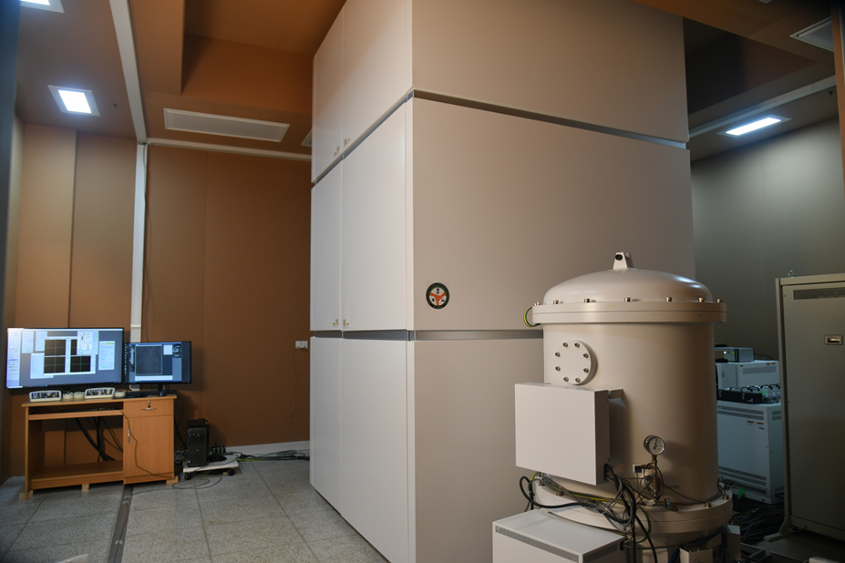
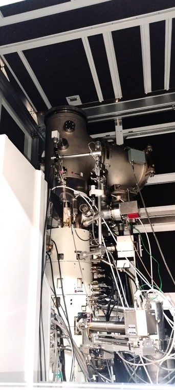
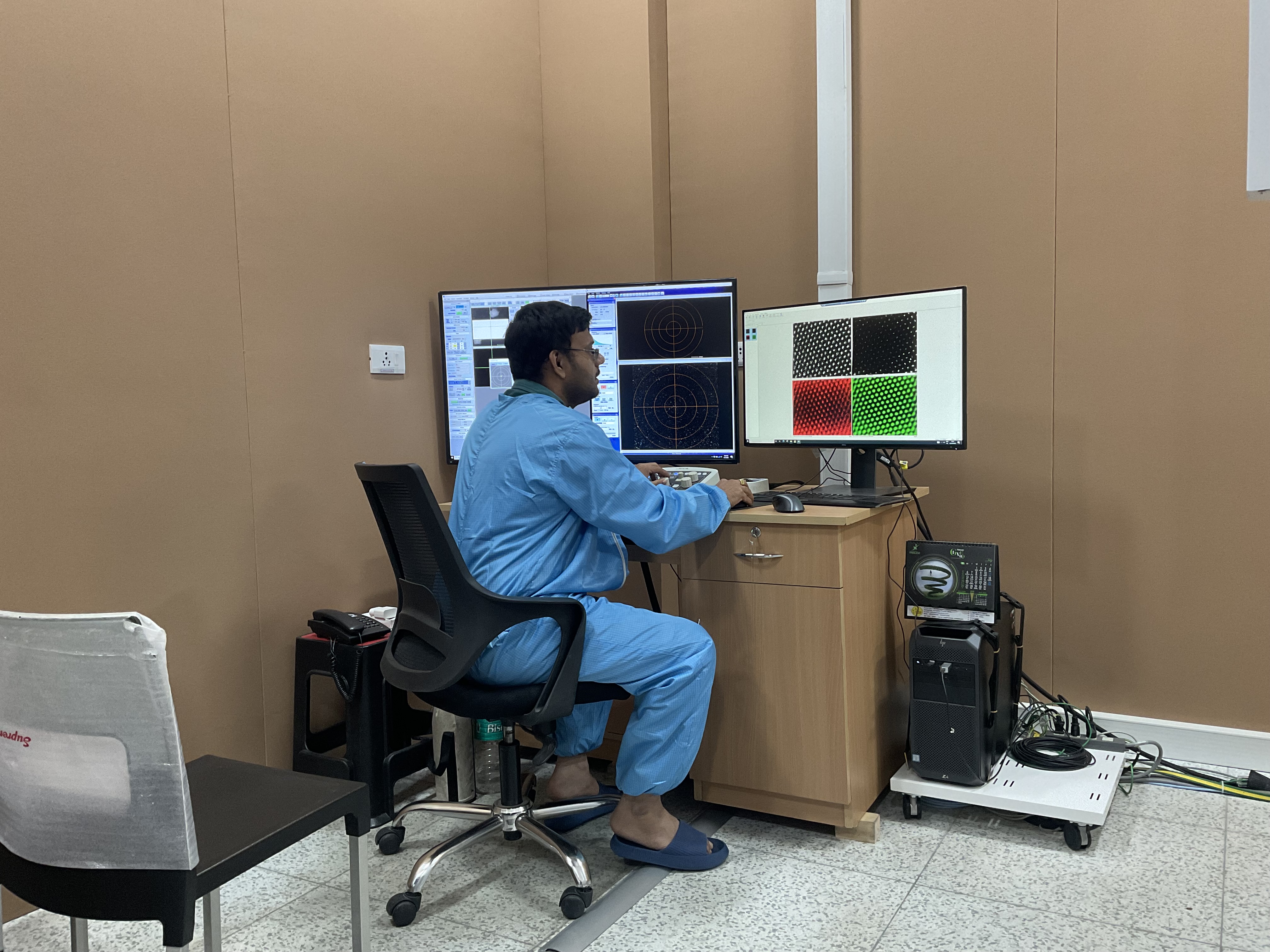
300 kV double aberration corrected (both image and probe corrected) atomic resolution transmission electron microscope (model JEM-ARM 300F2 GRAND ARM™ F2, manufacturer: JEOL, Japan) equipped with detectors for acquiring STEM (scanning transmission electron microscopy)-BF (bright field), ADF (annular dark field) and HAADF (high angle annular dark field) images, as well as spectra and elemental distribution maps using EDS (energy dispersive spectroscopy) and EELS (electron energy loss spectroscopy), using which one can obtain information about the structure (microstructure and crystal structure) and composition of a given material (including metals and alloys, ceramics, semiconductors, polymers, composites, functionally graded materials, rocks and minerals, thin films and coatings, nano-particles and 2D materials) can be obtained at different length scales ranging from micrometer to angstrom units. The HRTEM lab at SATHI has plasma cleaner to remove hydrocarbon contaminants from the sample surface as well as specimen preparation facilities including 3 mm disc-punch apparatus, ultrasonic disc cutter and precision polishing system. Procurement of a precision cutting machine, jet-polisher, and ultra-michrotome has been approved by DST, and is in process.
Understanding the properties of nanomaterials.
Semiconductor and quantum materials, including 2D materials.
Metals, including iron, steel, A, Mg and Ti based alloys, Ni based superalloys, intermetallics, high entropy alloys.
All kind of high-strength materials including diamond, ceramics etc.
Energy materials, including batteries and solar materials.
Studying materials for aerospace and defense applications.
To find the shape and size of materials.
Atomic arrangement of any material (with resolution of 50 pm or better), which is stable under vacuum and electron beam.
Crystal structure of materials.
Elemental composition analysis using EDX detector.
Elemental composition mapping using STEM-HAADF and EDX.
Atomic bonding and environment of atoms using EELS detector.
All these properties can be obtained under sub-nanometers scale.
1. Type of Analysis: The analysis modes are TEM / HRTEM / SAED / EDS / STEM EDS / EDS
Mapping / ADF / EELS
2. Sample Types
(i) Non-magnetic inorganic samples are allowed. For powdered samples that do not degas
under vacuum are allowed. However, sample preparation is a must for them.
(ii) Magnetic samples in powder form and organic samples are strictly not allowed
(iii) Sample types allowed are Powder (prepared on grid), self-standing film and disc.
(iv) For compounds and alloys containing magnetic elements such as iron, cobalt and nickel, the
user should provide couple of FESEM images of the powder sample (along with EDSpreferred) prepared on grid.
3. Sample size
For the HRTEM (High-Resolution Transmission Electron Microscope), the acceptable sample size
typically depends on several factors related to the specimen holder and the specific capabilities
of the instrument. Here are some general considerations:
Grid Size: HRTEM instruments like the JEM ARM 300 F2 often use standard TEM grids for sample
mounting. The most common grid sizes are:
Standard Size: 3.05 mm in diameter with a mesh size of 100 to 400 mesh.
Sample Thickness: The sample thickness should be suitable for transmission electron
microscopy (TEM) analysis. Typically, samples should be thin enough to allow electrons to pass
through for imaging and analysis. For thin films, thicknesses are often in the range of tens to
hundreds of nanometers.
Compatibility: Ensure the sample grid and holder are compatible with the JEOL JEM ARM 300 F2
HRTEM stage and holders.
Sample Preparation Guidelines
Proper sample preparation is crucial to obtain accurate and meaningful results. Here are
the sample preparation guidelines for various types of samples:
(i) General Sample Preparation Considerations:
Cleanliness: Ensure that your sample is free from dust, contaminants, and
residues.
Thin Sections: For TEM analysis, samples should be thin enough (typically <100
nm) to allow electrons to pass through.
Stable Mounting: Mount the sample securely on a TEM grid or holder.
(ii) Material Science Samples:
Polishing: Polish bulk materials to achieve a smooth surface.
Ion Milling: For cross-sectional analysis, use ion milling to create thin lamellae.
Replica Technique: Create a replica of the sample surface using a carbon film for
shadowing.
(iii)Nanoparticles and Nanomaterials:
Dispersion: Disperse nanoparticles in a suitable solvent.
Deposition: Deposit a drop of the dispersion onto a TEM grid.
Drying: Allow the solvent to evaporate, leaving the nanoparticles on the grid.
(iv) Inorganic Crystals and Thin Films:
Sectioning: Cut thin sections using a diamond knife or focused ion beam (FIB).
Ion Milling (Optional): Thin the sample further using ion milling.
Kindly note that specific sample preparation steps may vary based on the material type,
research goals, and the specific analysis you intend to perform.
Drop casting for powder samples (nanoparticles and nanomaterials)
(i) For the drop casting of the sample, the sample should be dispersed in isopropyl alcohol
a. In case of any challenges with isopropyl alcohol, then Acetone or distilled water can
be used
(ii) Sample (Metal disc / after drop casting on the grid) must be oven dried for 1 day.
a. Temperature depends on the type of sample (User need to take care of the
morphology of the sample)
(iii) Put the sample overnight in the desiccator before the day or two of the analysis
(iv) Bring the sample along with the desiccator for analysis
(v) Users requiring sample preparation services from the SATHI Foundation IIT Kharagpur need
to indicate or mention the same in the communication
(vi) A demo video is available on YouTube https://www.youtube.com/watch?v=rVT98ywELvE
1. External/Internal and Industrial users are required to prominently acknowledge the technical support/publication/financial aid arising from the facility in all publications/media releases and in the introductory paragraphs of annual reports while and after using the SATHI-IIT Kharagpur facility.
2. Do the registration with the link provided on the website prior to any payment.
3. Before sending keep every sample and reagent vial labeled properly with date. Unlabeled samples/reagents would be discarded.
4. In case of any technical query, please enquire/contact only coosathi@iitkgp.ac.in
1. Do not make the payment before final confirmation of your bookings.
2. Users are not allowed to enter lab or touch any equipment, chemicals or other materials in the laboratory area until you are instructed by lab in-charge.
3. Do not wander around the instrument facility, distract others or interfere with the laboratory experiments.
4. Any edibles, drinkables, and smoking are strictly prohibited.
5. Do not use the phone or laptop inside laboratory.
6. Do not use a flash drive on lab computers. For the data of your samples will be shared through mail or google drive.
7. Unauthorized experiments/samples are not allowed in the laboratory.
8. Users are not allowed to work in laboratory/facility premises alone or without permission of the COO, SATHI-IIT Kharagpur.
