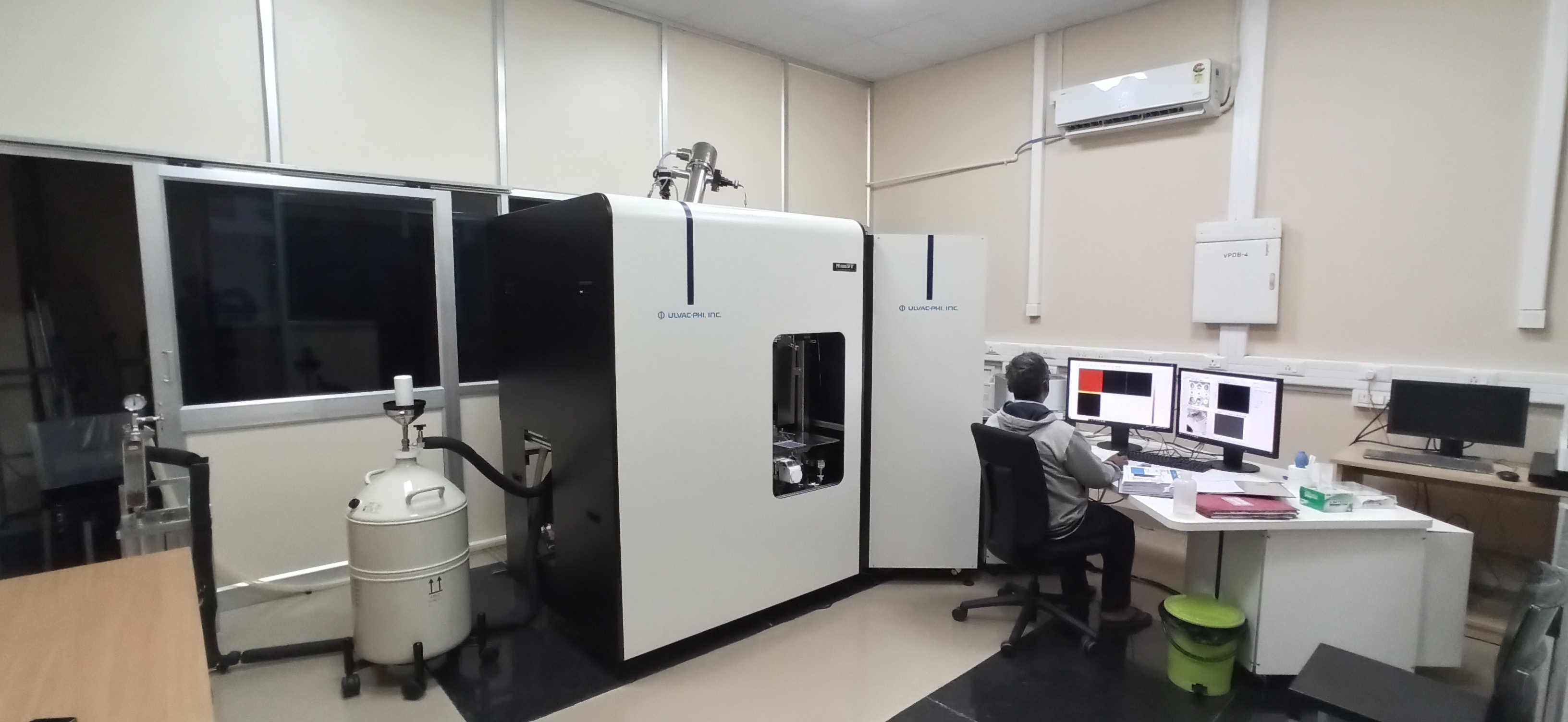
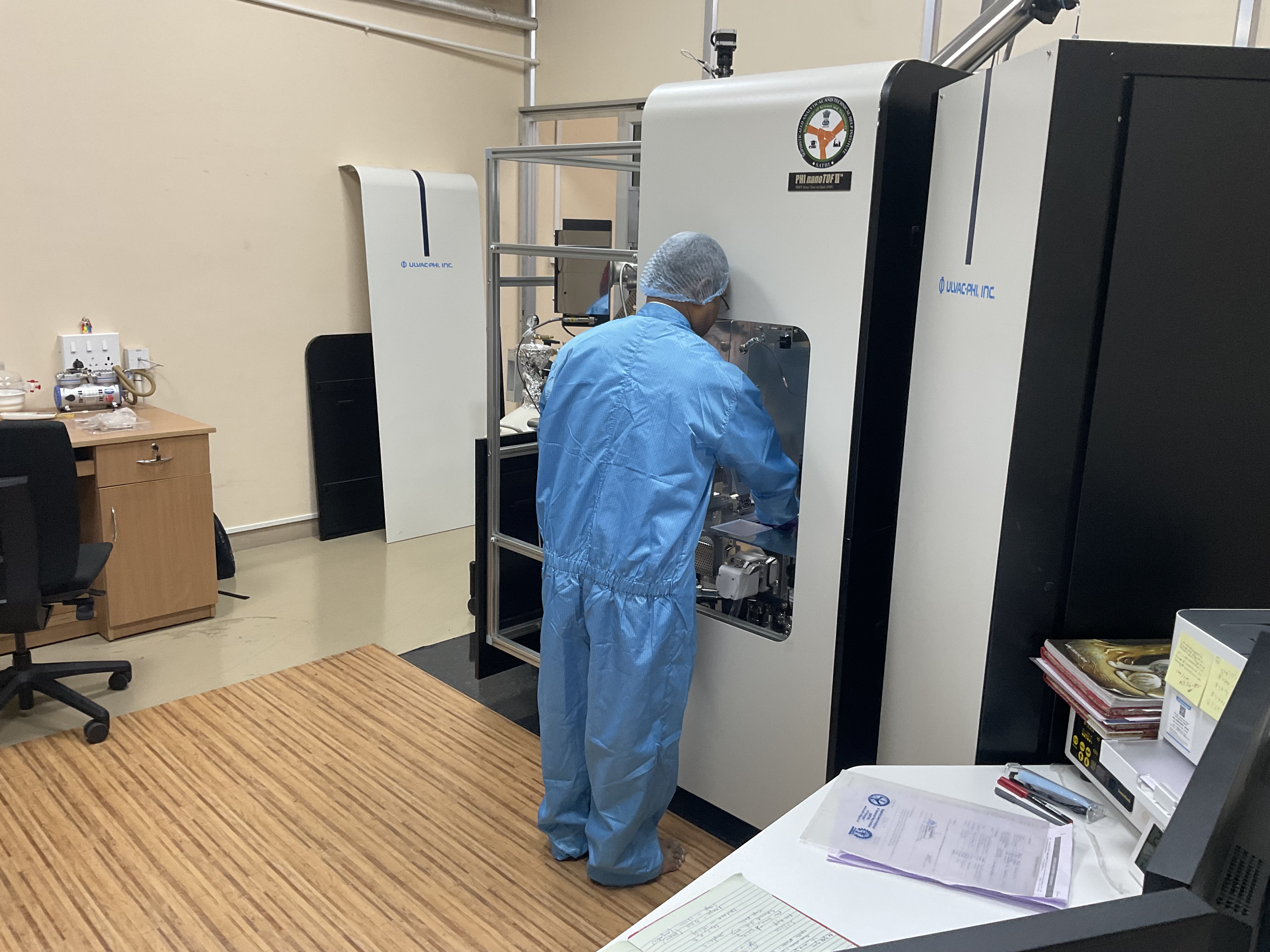
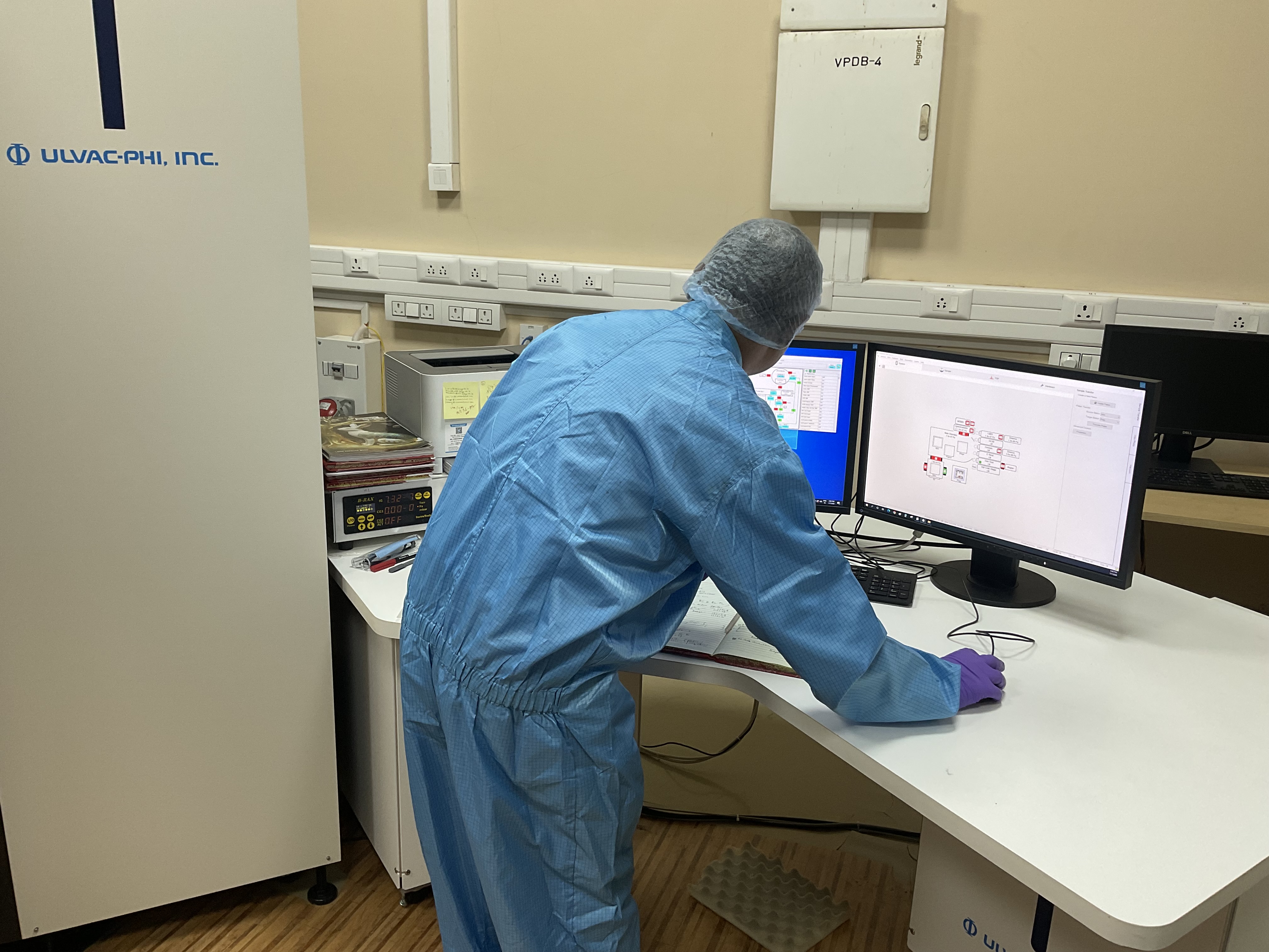
Time-of-flight secondary ion mass spectrometer (ToF-SIMS, model PHI nanoTOF II, manufacturer: Physical Electronics, USA) equipped with a parallel imaging MS/MS spectrometer, which can be used to obtain compositional information (mass spectra and 2D elemental distribution maps) of the surface within a depth of 5 nm as well as 3D elemental distribution profiles and maps along the depth ranging from 5 nm to 300 nm by depth profiling using in-situ argon ion sputtering. Surface enrichment of all elements mentioned in the periodic table starting from hydrogen can be detected. Additionally, a stylus profilometer (model Alpha-Step D600, manufacturer: KLA Instruments) is also available to measure the depth of surfaces after subjecting to depth profiling. The types of materials which can be examined include metals and alloys, ceramics, semiconductors, polymers, composites, and functionally graded materials in bulk form (which may have surfaces subjected to oxidation or corrosion, or hardening by carburizing, nitriding or ion implantation), multilayered thin films, 2D materials and coatings, as well as rocks and minerals.
Nano-TOF-II from ULVAC-PHI, along with a stylus profilometer (manufactured by KLA Tencor)
Widely used in many industrial fields viz: ceramic, lab-grown diamond, battery, medicine, resin adhesion, polymer, fiber, defect on display, BGA, Cu/Pl electric circuit, via hole etc.
Applications
Surface composition analysis.
Analysis of corrosion & oxidation
Quality control.
Research.
Reverse engineering etc.
Field of Utilization
Semiconductors, Microelectronics, Thin film and coatings, Metal, Polymer, Plastics, Pharmaceuticals, Biology etc
The acceptable sample types typically include:
(i) Solid Surfaces: This includes a wide range of solid materials such as metals, semiconductors,
ceramics, polymers, and thin films.
(ii) Coatings and Thin Films: Samples with coatings or thin films are suitable, as ToF-SIMS is
particularly useful for depth profiling and characterization of thin layers.
(iii) Organic Materials: Organic samples can also be analyzed, including biological samples (though
preparation methods might vary).
(iv) Composite Materials: Samples consisting of multiple layers or materials can be analyzed to
characterize interfaces and layer compositions.
(v) Semiconductors and Electronic Materials: ToF-SIMS is often used in the semiconductor industry
for process control and failure analysis.
(vi) Polymer Films and Coatings: Polymers are commonly analyzed due to their diverse chemical
compositions and surface properties.
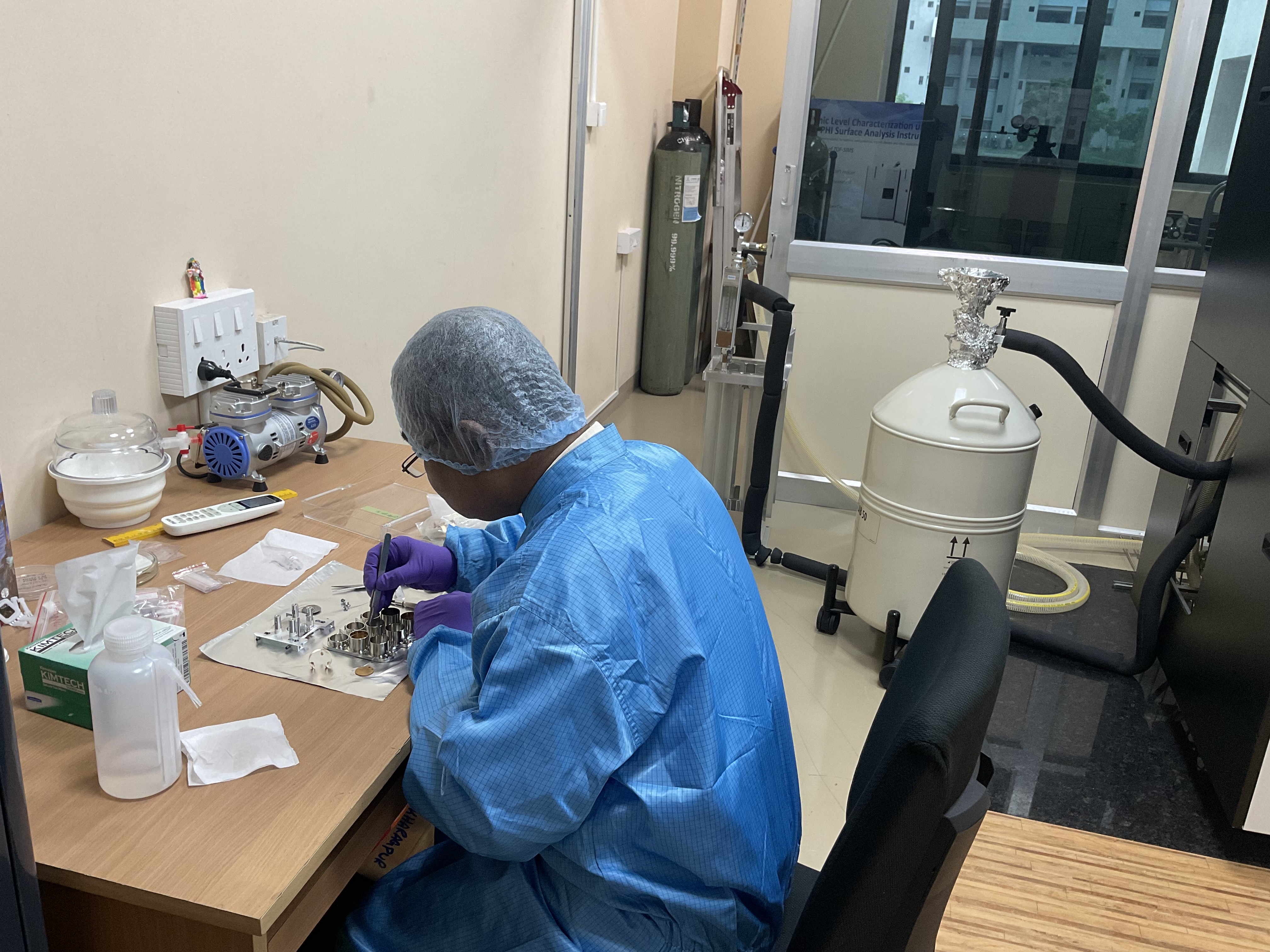
Before analysis, it's crucial to ensure that the sample preparation is appropriate for ToF-SIMS analysis,
which typically involves cleaning the surface to remove contaminants and optimizing the surface
condition for accurate analysis
The sample preparation steps for submitting a sample for ToF-SIMS analysis can vary depending on the
type of sample being analyzed. Here's a breakdown of sample preparation steps tailored to different
types of samples commonly analyzed using ToF-SIMS:
(i) Solid Surfaces (Metals, Semiconductors, Ceramics)
Cleaning: Clean the surface thoroughly to remove contaminants using solvent cleaning
(e.g., acetone, isopropanol) or plasma cleaning.
Drying: Ensure the surface is completely dry to prevent water or solvent residues.
Mounting: Secure the sample on a suitable holder ensuring stability during analysis.
Surface Smoothing: Polish or flatten the surface if necessary for improved analysis
resolution.
Masking: Use masking techniques if specific areas need to be analyzed separately.
Storage: Store in a clean environment to prevent contamination before analysis.
(ii) Polymer Films and Coatings
Cleaning: Remove any surface contaminants using mild solvent cleaning or plasma
cleaning.
Drying: Ensure thorough drying to avoid solvent residues.
Mounting: Secure the film or coating on a suitable substrate or holder.
Surface Smoothing: Flatten or ensure uniformity if necessary for accurate analysis.
Masking: Use masking if analyzing specific regions of the film or coating.
Storage: Store in a clean, controlled environment to prevent contamination.
(iii) Organic Materials (Biological Samples, Polymers)
Cleaning: Clean gently to avoid damage using mild solvents or detergents suitable for
organic materials.
Drying: Ensure gentle drying to avoid structural damage.
Mounting: Handle delicately and mount on a suitable substrate or holder.
Surface Smoothing: Ensure the surface is flat and uniform if necessary.
Masking: Use masking to isolate specific areas of interest.
Storage: Store in appropriate conditions to maintain sample integrity.
(iv) Semiconductor Devices and Thin Films
Cleaning: Clean with solvents suitable for semiconductor materials or use plasma
cleaning.
Drying: Ensure thorough drying to remove any residues.
Mounting: Secure on a suitable holder for stability during analysis.
Surface Smoothing: Polish if necessary for improved surface analysis.
Masking: Use masking for specific areas or features.
Storage: Store in a controlled environment to avoid contamination.
Additional Considerations:
Sample Conditioning: Some samples may require specific conditioning (e.g., annealing)
to stabilize or enhance surface features.
Documentation: Label samples clearly with relevant information (e.g., sample type,
preparation steps) for traceability.
Consult Manufacturer Guidelines: Always refer to manufacturer’s ToF-SIMS instrument
manual or guidelines for specific recommendations tailored to your sample type and
analysis goals.
By following these tailored sample preparation steps, you can ensure that your samples are
optimized for accurate and reliable analysis using ToF-SIMS instrument, regardless of the
material type being analyzed.
1. External/Internal and Industrial users are required to prominently acknowledge the technical support/publication/financial aid arising from the facility in all publications/media releases and in the introductory paragraphs of annual reports while and after using the SATHI-IIT Kharagpur facility.
2. Do the registration with the link provided on the website prior to any payment.
3. Before sending keep every sample and reagent vial labeled properly with date. Unlabeled samples/reagents would be discarded.
4. In case of any technical query, please enquire/contact only coosathi@iitkgp.ac.in
1. Do not make the payment before final confirmation of your bookings.
2. Users are not allowed to enter lab or touch any equipment, chemicals or other materials in the laboratory area until you are instructed by lab in-charge.
3. Do not wander around the instrument facility, distract others or interfere with the laboratory experiments.
4. Any edibles, drinkables, and smoking are strictly prohibited.
5. Do not use the phone or laptop inside laboratory.
6. Do not use a flash drive on lab computers. For the data of your samples will be shared through mail or google drive.
7. Unauthorized experiments/samples are not allowed in the laboratory.
8. Users are not allowed to work in laboratory/facility premises alone or without permission of the COO, SATHI-IIT Kharagpur.
